What is the basic structure of PCB design?
 14 Jan 2026 18:13:51 GMT
Tyson From www.hycxpcba.com
14 Jan 2026 18:13:51 GMT
Tyson From www.hycxpcba.com
The basic structure of PCB design mainly includes the following three core layers,
which together constitute the complete functional system of the circuit board:
Conductive Layer
This is the core part for realizing circuit functionality, usually made of copper foil. The copper foil is processed through etching.
Conductive layers can be divided into signal layers (such as top layer and bottom layer) and reference planes (such as power and ground layers).
Signal layers are used to transmit electrical signals, while reference planes (power and ground layers) provide low-impedance return paths for signals.
In multilayer boards, signal layers and reference planes need to be closely paired to reduce interference.
Insulation and Protective Layers
Substrate Layer (Insulation Layer): Typically made of insulating materials like FR-4, this layer provides physical support for the circuit board and ensures electrical isolation.
Solder Mask Layer: An insulating coating (such as green solder mask) applied to non-soldering areas to prevent short circuits and oxidation.
Silkscreen Layer: A text layer used to mark component designators, outlines, and other information, facilitating assembly and maintenance.
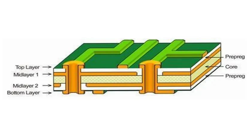
Substrate and Laminate Structure
The PCB laminate design is achieved by alternating stacking of cores and prepreg (PP) sheets. The core is a rigid double-sided copper-clad substrate that can serve as a signal or power layer.
Prepreg is used to bond the layers together and is non-conductive. The laminate must be symmetrically designed (such as for an even number of layers) to prevent warping. For example,
a 6-layer board structure might be: signal layer - ground layer - signal layer - power layer - ground layer - signal layer. Multilayer boards achieve inter-layer connections through vias, blind vias, or buried vias.
By reasonably designing the laminate and layer distribution, signal integrity, power stability, and manufacturing costs can be optimized.

-
06 Mar 2026 14:08:44 GMT
What is Heavy Copper PCB
-
04 Mar 2026 10:15:22 GMT
How Dose AOI Enhances Solder Paste Inspection For PCB