How to Choose Correct Wireless PCB with Project
 31 Jan 2026 11:07:55 GMT
Tyson From www.hycxpcba.com
31 Jan 2026 11:07:55 GMT
Tyson From www.hycxpcba.com
Wireless on Printed Circuit Boards revolutionized modern-day electronics, where information can be shared between devices sans cables. Thus, the advanced integration of one circuit board into wireless technologies like Wi-Fi, Bluetooth, and RF greatly enables the ease with which devices connect.
Starting from smartphones to smart homes, and reaching industrial automation, this technology is immensely useful in improving mobility, efficiency, and connectivity. This includes wireless PCBs, which, in the near future, are going to become much smaller and more power-efficient, very adaptable for each and every device of the modern connected world.
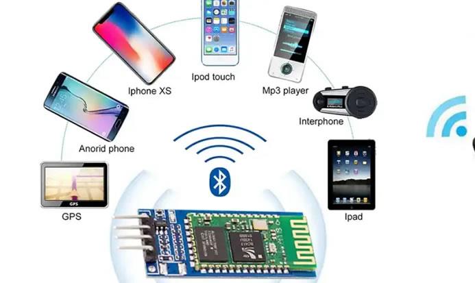
What is a Wireless PCB?
This would also include Wi-Fi, Bluetooth, NFC, and RF communications. The areas where the usage of their application is noticed include smart devices, IoT applications, and industrial automation. This is because it permits increased flexibility in device design, reduction of cable clutter, performance, and efficient power consumption.
The Role of Wireless PCBs in Modern Electronics
Reduces Clutter, Enhances Portability
Smarter Connectivity
Improvement in IoT Communication Devices
Promotes Comfort to the User
Accommodate Advanced Applications
And since wireless technology isn’t going anywhere, wireless PCBs will forever be in developing the future of smart and connected devices.

The Technology Behind Wireless PCBs
Wi-Fi
Bluetooth
RF
NFC
Zigbee and LoRa
Common Wireless PCB Applications
-
Consumer Electronics: Wireless PCBs have powered such innovations as smartphones, smartwatches, earbuds, and controllers that are designed for easy and seamless connectivity with the users.
-
Smart Home: Many of the devices in a smart home, such as smart thermostats, security cameras, and automated lighting systems for energy efficiency, can be controlled from a distance.
-
Healthcare Devices: Wearable medical gadgets, wirelessly capable patient monitoring systems, and smart implants are devices needing wireless PCBs to operate in real time and send on data for remote healthcare support.
-
Automotive Sector: Some of the major applications of wireless PCBs include GPS navigation systems, keyless entry, infotainment, and ADAS to make vehicles more functional in an attractive way.
-
IoT: These include wireless sensors and monitoring devices, which reduce manual interference in the automation of manufacturing, monitoring, and optimization processes.
-
Smart Agriculture: Wireless PCBs find their application in IoT-based farming equipment, including automated irrigation systems, soil moisture sensors, and remote weather monitoring devices.
Challenges in Designing Wireless PCBs
Signal Interference
Power Consumption
Heat Management
Antenna Placement
Miniaturization and PCB Layout
Regulatory Compliance
How to Choose the Right Wireless PCB for Your Project
Connectivity Requirements
Power Efficiency
Size and Form Factor
Environmental Conditions:
Antenna Integration:
Regulatory Norms:
Cost Versus Manufacturing
Conclusion
Designing an effective wireless PCB demands the solving of some challenges related to signal interference, power consumption, and regulatory compliance. Wireless PCBs will be selected based on connectivity requirements, power efficiency, and operating conditions. In the future, wireless PCBs will continue to drive innovation in making devices smarter, smaller, and highly efficient in a connected world.
-
06 Mar 2026 14:08:44 GMT
What is Heavy Copper PCB
-
04 Mar 2026 10:15:22 GMT
How Dose AOI Enhances Solder Paste Inspection For PCB